Quantcast
Channel: Amplifiers forum - Recent Threads
Viewing all 18769 articles
Browse latest View live

Very Very low Charge and Current measurments circuit design for Ion chamber Measurments.

$
0
0

Hi Paul Grohe,


I would like to design a Charge collection Circuit using the LMP7721 and IVC 102, to be connected to a Farmer Ion Chamber used in Radiation measurements. the measurement range should be from 5 femto amps (preferable) to about 10 Micro Amps.

I have only basic knowledge of Electronics and not very good at mathematics, however studied the evaluation boards of both these IC. I understand Noise and stray capacitance are a big issue at these level. I need to integrate both these cct,  and they should be working at floating levels of HV as the signal Input and the guard ring should be at HV level WRT to Ground as the chamber exterior is grounded.

These will be done with Timed measurements i.e. output will be measured with time, or free running depending on user, also the HV is going to be altered in polarity the voltage levels, to check polarity effects.

Can I get some help.


James Mazarello

India


IVC102 reset-and-integrate measurement:

$
0
0

I have acquired a BB IVC102 precision amplifier for detecting small currents originating from an ionization chamber.

In order to detect currents up to 100nA, I am integrating for 10ms before closing S2 for 10us and starting a new measurement. When I monitor V0 during 10 consecutive integration periods, the EVEN and UNEVEN voltage ramps are markedly different. For example, ramps 1-3-5-7-9 each reach 1V after 10ms, while ramps 2-4-6-8-10 each reach 0.65V.

The current provided by the ionization chamber is fairly constant and is certainly not expected to fluctuate with such a methodic behaviour, so I suspect this is a phenomenon introduced by the IVC102.

Any help explaining this behaviour would be greatly appreciated.

Thanks, Pieter

Strain gage and Temperature measurement with Instrumentation Amplifier

$
0
0

Hi all,

I've purchased INA122 to make a strain gage measurement. I have couple of questions. First of all, I'm very new to electronics and my questions may be very easy or basic to you but I really want to learn.

I want to make a quarter bridge measurement. How do I choose gain value for my strain gage output? I guess the idea is to make input range amplified to a level which ADC can process. How can I measure the maximum output of strain gage? Do I need to calculate the maximum voltage in a way?

Another thing is that I want to make a temperature measurement using a PT100 sensor (shown below). Do you have a specific component for this sensor? Or If I make a circuit in which the current is limited to 500 mA, than use an ADC, does it work for me? (For now speed and resolution is not problem for me.)

Thanks in advance, Regards,

Problem with INA333 testing circuit

$
0
0

Hello TI,

I've just got some INA333 samples from TI.

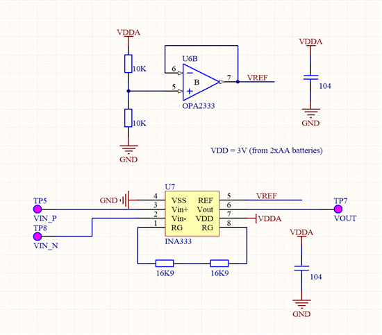
I made a circuit to test this, but  I have 2 problem.

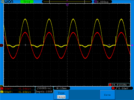
- Gain always = 2

- Positive signal is cut off.

Please take a look at the image below about the circuit and the signal from ossillo.

Channel 1 is signal from function generator( Amp = 500mV, f ~ 35Hz)

Channel 2 is out voltage from INA333. Vref ~ 1.5V

INA 163 - single supply

$
0
0

I´m using an INA163 (instrumentation amplifier) with a dual supply, +-5V. But, to get a better performance in my project, I don't want to use a negative source anymore. So, my idea is to connect V- to the ground. But, I tried it and the amplifier responds in a very strange output. I can't figure out why.

When I use the dual supply, my output is something between 3.5 and 4.8 V. Using a single supply, I expect a gap smaller than this. To be exact, the INA163's data-sheet says that there's a lost of 1.8 V in each side of source. So, my gap should be (5 – 1.8) – (0 + 1.8) = 1.4 V. My inputs are very similar, with a small variation of milivolts. The interval measured with dual supply shows me that this small one should be enough. But my output with single supply is always constant (4V) to a very different values of input.

The only change that I did in my circuit is the V- to the ground. I researched in INA163's data sheet looking for something about single supply, but there's anything. Also read a Texas' application report, A Single-Supply Op-Amp Circuit Collection, SLOA058, but I still can't find out what's is happening. Anyone have any idea what's happening?

Signal conditioning circuit for EEG acquisition.

$
0
0

Hello,

    I am working on development of signal conditioning circuit for EEG signal acquisition.

I got a problem with designed circuit, which is attached to this post.(Please visit the site to view this file)

I have used INA333 and OPA350 for designing the circuit. As you know both can work on single supply, i have given 3V as Vs and another one is grounded.

The problem is,

If i give single supply to INA333. signal is not getting amplified. The signal is getting amplified only on dual supply.

Please rectify my problem.

AN-1796 LMP7721 Evaluation Board

$
0
0


Hello , I have purchest recently an Evaluation Board containing the Op Amp LMP7712  and LMP7715 (LMP7721 Multi-Function Evaluation Board Users' Guide© 2009) ,

This evaluation board(http://www.ti.com/lit/ug/snou004/snou004.pdf)  is working with a triax cabels.

I am using there the non inverting option and i am conecting a resistor of 10k at the end of the triax cabel (about 40cm long with 180pf capcitance).

i trying to get a flat response of the noise of this 10k resistor till 100khz . eventualy i am measuring this noise at the spectrum but at about 70khz

the spectrum response rise , i guess from peaking of one of the amplifiers . i have tried to put the Cf capcitor to lower the bandwidth but this didnt work,

i also tried to build it with different amplifers with higher GBW, the response have improved but still i have peaking.

also tried without the feedback amplifer LMP7715 just connecting the inverting leg to the guard shield but still there is peaking.

may i add that as the cable is longer the response rise earlier , also i rise the value of the resistor.

i will happy to recieve an advise.

Thanks


INA321 multiplexing

$
0
0

Hi,

first post so forgive me any lapses in etiquette!

I see in the datasheet for the INA321that pulling the shutdown pin to 0V puts the device into shutdown mode and that the output impedance then goes high and therefore suitable for multiplexing..

I was thinking of using a 3 t0 8 line decoder to select which one of 8 INA321s to read...

My problem is that I don't have access to the shutdown pin as the amplifiers is located at the end of  3 core cables, next to their respective strain gauges.

can I get the outputs of the 7 devices  to go high impedance and therefore suitable for a  input to a single DA convertor by using the decoder to connect VDD or VSS to the INA321 instead of using the shutdown?

Chris


output impedance of LPV521 follower

$
0
0

Hello,

I have a question about LPC521 follower, we are using it with MSP430F5438A, the input is 3.8V and after a resistor divider, 1.9V feed to LPC521 voltage follower. and output to a analog input pin ( p6.0 )of MSP430F5438A, I notice the reading from multimeter at the p6.0 and the ADC value have a 80mV to 100mV difference( ADC reading are higher than multimeter) . we have other ADC reading from p6.1(1.5V DC) and p6.2 which are very close to the multimeter readings, that prove the reference should be OK. it turns out MSP430F5438A ADC require the output side impedance smaller than 10K(see MSP430F5438A errata, ADC 27 work around). I think the voltage follower should have low output impedance. but I am not sure about this LPC521.

I also notice if add a 0.1uF cap bypass LPC521 follower output to ground, will make the ADC reading close to multimeter. could anyone explain why this cap can make this happen. it is a DC voltage, and from the scope the ripple is very low. less than 20mV.

Sincerely,

David Sun

XTR111 DAMAGE ISSUE

$
0
0

Hi,

I'm now debugging my new design with XTR111, unfortunately the XTR111 is always damaged.

Here is my schematic.

Some times when I power on the board, then I found the chip XTR111 has been damaged.

Some times it seems work well, I can get a precious current output. Then I remove both the loads of regulator and the current loop, just power on the board and wait, several minutes later, the chip is damaged as well.

Is there anyone can give me some advice?

Thanks a lot.

Cloud Hu

GE Oil&Gas

Sense pin in INA2126

$
0
0

Hi 

I have designed ECG data acquisition using INA 2126. What is the sense pin stand for?

Thanks

Reza

08/20/13

INA326 Common-Mode and Differential Mode Limits for G=1 ?

$
0
0

The INA326 is presented as a true rail-to-rail input and rail-to-rail output instrumentation amplifier, and this seems to be the case for G=50. I would like to use it so I dont have to make an instrument amp out of 3 rail-to-rail op amps.

But is rail to rail i/o guaranteed for other gains? I am very used to losing rail-to-rail operation on inputs and/or outputs when using other instrumentation amplifiers at low gains, Maybe its because I have been using a different supplier. Usually the supplier gives a chart of output swing versus input common-mode for several different gains,a  fixed output load, and for many different supply voltages, but that is not in the INA326 data sheet.

Could an applications engineer take a quick look at the attached circuit diagram consisting of 3 resistors and an INA326 with G=1 inand tell me if I am still operating in the linear range of the part ?

(Please visit the site to view this file)

Basic RCV420 and XTR110 connections

$
0
0

Ok, I am trying to connect a XL-MaxSonar-WR1-MB7052 sensor from MaxBotixInc (which output is voltage from 0 to 5V) to the XTR110 and then the XTR110 to the rcv420 and read this voltage with ADC module of PIC 16F877A from microchip; could you tell me how should I connect the xtr110 and the RCV420 for this purpose?.

INA326 input bias/offset current appears much higher then spec

$
0
0

I am dealing with a design issue related to INA326. The circuit is attached.

(Please visit the site to view this file)

The input bias circuit is supposed to be set the negative input to 1.99V, while the positive input is set to 0.51V.

 However, when I probed on the positive input, I measured 0.88V instead, which is way off. The negative input is correct though, 1.99V.

 I lifted the positive input pin of INA326, then I measured 0.5V on the net.  But this time the negative input goes up to 2.513V.

 Then I lifed up the negative input pin, the net voltage became 1.99V.

Apparently, there is significant current, above 90nA, flowing out from the INA326 device, which is not specified in the datasheets. The bias current and offset current are what our design based upon, which are 2nA max. When you measure these current, do you actually have both negative and positive input at the same common mode voltage to measure, or you covered the case we are having, positive input is at 0.5V, and negative input is at 2.0V? If the circuit does inject 100nA current out, I’d like to know the range based on INA326 design.

 In the same time I tried to simulate this behavior, with knowing the model might not be able to provide any info. The problem I ran into is this.

 "Operating point  not found,

Component U3.J8"

Please see the attached the SPICE circuit  and see if you know why this happens, and if this is related to the issue.

 (Please visit the site to view this file)

Regards,

 Derek 

TLC272C and TLC2272C in voltage follower circuit

$
0
0

Hello,

My customer has been using following Opamps for monitoring back-up battery voltage as voltage follower configuration.

TLC272CPWR for previous model

http://www.ti.com/product/tlc272

TLC2272CPWR for new model

http://www.ti.com/product/tlc2272

Customer has recognized that new model (TLC2272C) consume more back-up battery power than previous model(TLC272C), then the back-up coin battery can not last longer than few month, this is quite short compare with previous model.

Then they  suspects that the input impedance during power-off state of each opamps are bit different, this means input impedance of TLC2272C is smaller than TLC272C, then draw more current from coin battery.

Do you have any data which express the differences on input impedance during power-off state?

One other thing, I suspect is leakage current via ESD diode.

If both devices have different protection circuit, then cause differ leakage current consumption.

Can you please also comment on this point as well?

It's really appreciated, if you can guide me what should we check.

---

  • TLC272CPWR for previous model
  • TLC2272CPWR for new model
  • Both circuit apply voltage follower configuration
  • battery voltage is 3.3V
  • Output of opamp is connected to ADC input

---

Thank you for your support in advance.

Regards,

Ken


OPA333 Single power supply

$
0
0

Hi All.

i'm making a inverter amplifier. i configure opam in single supply like application guide "Single-Supply Op Amp Design Techniques" i do it in bread board and simulation in Tina but output alway satturation, with in put is sine signal 0.01V. I don't know why it not work. I upload the schematic .

Thank for any help

Phitu.

(Please visit the site to view this file)


Pull up connection on LM2901D

$
0
0

Hi,

I planned to use LM2901D differential comparator in my design. Supply voltage is 24V and inputs to the comparator are also around 24V range. However I want to pull up the output by other supply voltage, say 3.3V. Is this ok?

I have rigged up the circuit and found the output voltage level changes as per input. But I could not get any information regarding pull up voltage level from the device datashet.

Also, I could find  LP2901D datasheet saying that pull up voltage level is independent of supply voltage, please refer to page no. 5 of device datasheet.

( "An output pullup resistor can be connected to any available power-supply voltage within the permitted power-supply range, and there is no restriction on this voltage, based on the magnitude of the voltage that is supplied to VCC of the package.")

So please advice whether LP2901D could be better for this requirement.

Best Regards,

Rajesh

Which technology process used for INA212?

$
0
0

Which technological process used for INA212 - CMOS or bipolar?

Regards

Alex

RCV420 short circuit in its inputs

$
0
0

Hi,

I don't find any information in the datasheet of the RCV420 about the possible short circuit of the side of the current loop.

Is it destructive for this component ? So, we must use a particular protection.

I don't find any information about its current consumption. Did you have this informations, nominal and extrem with the temperature.

Many thanks,

Best regards,

Pascal

AMC1100 Rin specs?

$
0
0

The AMC1100 datasheet specifies a differential input resistance Rin=28kOhm. What are its minimum and maximum values and how does it change for a wide range of operating conditions such as supply voltage and temperature?

Viewing all 18769 articles
Browse latest View live


<script src="https://jsc.adskeeper.com/r/s/rssing.com.1596347.js" async> </script>