I plan to have a pull-up resistor on the Discharge pin to a voltage higher than Vdd (for level shifting).
What is the maximum voltage allowable on the Discharge pin ?
Is the Discharge pin internally clamped to Vdd?
I plan to have a pull-up resistor on the Discharge pin to a voltage higher than Vdd (for level shifting).
What is the maximum voltage allowable on the Discharge pin ?
Is the Discharge pin internally clamped to Vdd?
I have Buf01900 http://www.ti.com/lit/ds/symlink/buf01900.pdf, that I have hooked up to DEO Nano with 3.3 VD with I2C. Tested my I2C on board and off board. Its just not ack its address or all clear. Does someone have experience with working on the Buf01900?
In looking at the PGA309 user guide, table 1.1, the Zero Offset adjustment capability is stated as +/-200%FS (coarse and fine combined). I assume FS means the full scale output of the sensor, in mV. However, it seems like the offset adjustment should be more. +/- 48mV coarse offset, and an additional fine offset adjust from the ZeroDAC of up to 4096mV/input-stage-gain (RTI). Is there a limitation I'm missing? Thanks for your help.
Can a LM331 frequency to voltage converter work with a sine wave input?
Hello,
I have built a 70X gain Diff amplifier usiing LMP2012 for a thermocouple. It
performs well except for an input offset. Having 2K input resistors and connecting a
thermocouple creates 20mV input offset. Seeing as I have used a single power supply
negative trimming is an issue and LMP2012 does not have a offset pin.
(Please visit the site to view this file)
I assumed that the 36uV offset advertised would be the one present on my input. Was this an
error and is there a simple fix.
NOTE: using dual package opamp for 2 channels.
What is the difference between specification temperature range and operating temperature range? For e.g INA 121 has a specification range of -40 to 85 C and a operating range of -55 to +125 C
Best Regards,
Kavindu
Hi Paul, I saw your amazing YouTube video: http://m.youtube.com/#/watch?v=n90whRO-ypE&desktop_uri=%2Fwatch%3Fv%3Dn90whRO-ypE
...showing you can accurately weigh an Eyelash hair. I am carrying out a study for an international Conference for Eyelash Extension professionals and have been searching everywhere on how to accurately weigh various combinations of individual Eyelash Extentions. Can you advise me on how I could access something like that? Even to hire or something? My partner is a Electrical engineer so he should be able to help but any advice would be grately appreciated.
The forum that I post on for Eyelash professionals were even considering pitching together to buy a suitable scale (to answer our many questions about this for Natural lash safety) but they're extremely expensive from what I've heard.
Any advice you ( or anyone else) has I would be most grateful.
I would really appreciated if i get some help on the below topics
I am designing a non contact ECG sensor to display ECG signals in an oscilloscope. The basic design would be having two electrodes to pick up the signals and then some signal processing scheme to filter off noise and probably a DRL circuit as well. Could you suggest suitable componets availabe for this & any design recommandation to this work?
Hi Guys!
I need some technical help in answering the below:
The application has an encoder which has a differential output and it is buffered then amplified (put in mid rail and filtered), see channels A,B,R in the below schematics. The question is, can the buffer stage be removed? (see app.note SPRA496).
Instead of the buffers we want to use a 120ohm termination resistor and remove the buffers. Do you think it can be done? Or there may be impedance mismatching?
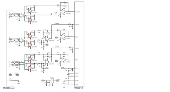
For differential analog line interfacing (HEIDENHAIN for example, used for sin-cos encoder, up 10meter cable lenght): would you consider using this high impedance buffered interface for analog signal, or a 120Ohm termination resistor and more simple low cost interface as depicted below?
Please advise,
Thanks,
Gianni
I'm using a LMP2232 as a buffer to monitor 2 28vdc signals. The device has failed and with no input 1 channel has 1.5v on the output and the other channel has 0.13v.
Both circuits consists on a 10:1 voltage divider (88.7k and 10k) feeding the input, with the device configured as a voltage follower and it's output going to an ADC input of a MCU. Vdd = 3.3v
Question is what could have caused this failure and how do I protect against it?
Can this Dual Variable Gain Amplifier (VGA2615, VGA2616) be used in fully differential mode?
Since the the VGA essentially contains a Low Noise Preamplifier followed by Voltage Controlled Amplifier, can the input to LNP be differential? Because in the typical circuit diagram and evaluation schematic, the LNP is always used in single ended configuration.
Also give details about the biasing. Can the internal bias of the IC(Vcm) be used to shift the output common mode(Vocm) of the front end amplifier (THS4131) just before the VGA?
On the TL331KDBVR comparator, how do the device parameters vary at VCC = 3.3V? All characterization data in the datasheet is at VCC = 5V.
How do I change registers in the PGA309EVM software (Rev. C). On the block diagram, I click "Write all Reg". The block diagram and register screens change, but the device doesn't change operation. The autocal and EEPROM screens don't show any change, either. "Read all reg" brings back the old register values. Power off/on after "Write all Reg" doesn't work, either. No new EEPROM file is created.
I'm trying to change the coarse offset, so maybe there's another way. Autocal always gives me maximum negative coarse offset (not needed for my sensor: 0-60 mV.). This solution, of course, gives me maximum clock noise. Can I get autocal to reduce coarse offset?
Thank you.
Hello,
I am trying to use the XTR300 as a constant current source in order to measure impedance across tissue using a 1V p-p sine wave as the input. The circuit diagram can be found below. However, when measuring the voltage across the tissue, unplugging the leads (creating an open circuit from DRV to ground) results in the presence of a constant AC voltage. Shouldn't this value be zero, because no current should be flowing? What could be possible causes for this?
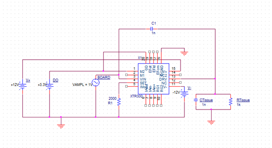
Thanks,
Tanner
Hi everyone, I'm studying in deep a circuit I've found in a TechNote of Texas Instruments(amplifier for electret microphone) for my "Sensors and Transducers" examination. Could I know how describe the filtering operations and the filters model used in the two stage (with opa140) of the circuit? I didn't understand so well the explanation. This is the comment in the description: "This single-supply +5 V circuit uses both op amp channels to provide a total of 40 dB of gain (20 dB/stage) in combination with second-order high-pass and low-pass filters.....Low-pass filters are formed by combining the feedback capacitor and feedback resistor, which sets the cutoff frequencies to fc = 1/(2piRC). High-pass filters are formed by combining the amplifier’sinput impedance and the input capacitors setting the cutoff frequencies to fc = 1/(2piRC).A high-frequency low-pass filter is formed by combining the ECM load resistor and C3,the 33 pF shunt capacitor...". I insert the image of the circuit.
(Please visit the site to view this file)
regards, Vincenzo.
Problem:
*LM339 not switching when input voltages are close to each other(i.e. 2.62Vref on inverting ) and 2.8V on non-inverting input)
* Open collector output of the LM339 is pulled to +5V through a 10K resistor; When inverting input gets 187mV applied, with 2.8V present at non-inverting input , the LM399MX/NOPB operates as intended(i.e. open collector output gets pulled up-to +5V).
However, when Vref/inverting input = 2.62V, with the 2.8V still at +Vin, The LM399MX/NOPB output stays LOW. The IC does not seem to be discerning 180 – 200mV input difference.
Is there some internal hysteresis that we don’t know about…?
Digikey’s specifies the LM339MX/NOPB as a General purpose LOW power comparator type.
They also have the LM139ADwhich is of a Differential type.
I am confused as to what the difference (if any) is between a general purpose LM339 and a differential LM339.
I need the comparator’s output to float to +5V under both non-inverting input voltage (187mV & 2.62V) conditions.
Please advise on a viable alternative.
Thanks
Mamadee V. Fofana
Contract Embedded Systems Design/Development Engineer
I am designing a motor driver circuit for a product I am designing using the OPA549. Straight forward common design.
Problem is even at low currents (0.5 to 1 Amp) the OPA549 quickly heats up to thermal shutdown (I have a heat sink on the chip). The circuit configuration is a typical non-inverting op-amp configuration using 5.1k/13k (a gain of about 3) resistors for feedback on the negative input. Power supply is from a 12 volt battery and is decoupled at the chip with the recommended 10uf and 0.1uf capacitors. Basically my circuit is nearly identical to the application notes recommendations.
The output of the amplifier has a 0.25 ohm power resistor and I replaced the motor with a 1 ohm power resistor for test purposes. The input to the amplifier is from a DAC on a microprocessor. Ideally I will be driving the motor with a sine wave at about 6v p-p at <400hz and at about 4 amps rms.
With an ammeter on both the power input and the current through the output, at only 0.5 amps the op-amp heats up very fast, but I am only seeing the expected 0.5 amp of current at both points. I set the input at a dc voltage so the output is dc. Even with a sine wave drive the chip heats up. Looking at power, inputs, outputs,... with my oscilloscope I do not see any oscillations.
Seems to me that the chip should not get that hot at only a half amp of current.
I am stuck as to what else to check. Any suggestions?
Hello, I'm wondering could you add INA125UA to samples list? Or any other INA125 in SOIC package? Now, on place where "Free Sample" button should be, says "Contact TI Distributor or Sales Office". I would really appriciate this if you could make it happen because I'm designing my whole PCB to be in SMD. And I just want to say that I really appriciate your Free Sample program, and I think it's a great way to help out students like myself. Thank you and have a great day!
Dear Sir/Madam,
I'm planning to use PGA280 in my design.I'm want FITs data of PGA280 to calculate the MTBF of my board .
Kindly do the needful.
Regards,
Venkatesh
what is the difference between the 2 Products LCD Gamma Buffer and Operational Amplifier (Op Amp) ?