I have a signal that varies between 19V and 17V @ 250kHz. The signal operates in a burst pattern where it outputs 2048 values then stops for a few ms. I want to input this signal into an op amp and remove the dc level. I have a circuit that has a dc blocking capacitor between the signal and the op amp input. The op amp is set as a buffer, and also has a resistor to ground. So I have a high pass filter on the input of the buffer. The issue I have is that I am finding that the circuit takes a long time to settle if I select values that maintain the signal integrity. If I then change the values to speed up the settling time the signal starts to degrade. Are there any other options that will maintain the signal integrity whilst giving a fast settling time? I am open to using a completely different circuit. Thanks
↧
remove dc offset from signal going into an op amp
↧
LMP8481: LMP8481-H at voltages less than 10V and low Rload values
Part Number:LMP8481
At 5V and low Rload, gain is low. Vcc is connected to Rsense as in your typical application schematic, page 1 of datasheet.
My schematic Rsense= 0.1 ohm, RefA and RefB are grounded, unidirectional current flow
Typical Iload= 1A, Rload= 4.9 ohms with measured Vsense= 0.1V
Vout should be 10V. It's a lot lower, about 6V (gain no longer 100X) Increasing Rload to 10 ohms gives correct results.
If I disconnect Vcc from Rsense and bring in Vcc externally, circuit works at 5V/1A if powered with Vcc= 12V.
Am I missing something when interpreting the datasheet? As a minimum, I need a criteria for changing to external Vcc.
Thank you.
↧
↧
INA282: Application Question Consultation
Part Number:INA282
Hi,
I have some questions about INA282 application:
Supplement the customer application scenario: when the current is from left to right,
To output a high level (greater than 1V);
When the current is 0A and is from right to left,
To output a 0V voltage or a voltage less than 0.5V; used to solve the current backflow of the PMOS tube.
1. What is the range of differential voltage values across the sampling resistor?
2. What is the GAIN gain value to do?
3. What is the calculation formula for the sampling current and output voltage?
4. If the unidirectional current is connected from left to right, what state of the output voltage is when the current is from right to left in actual use, and what state will be if the detection current is 0. ?

thanks.
↧
OPA2210: About AD8676 replacement, OPA2210, OPA2192, OPA2191
Part Number:OPA2210
Dear Ti Community,
I want to replace a force and sense buffer as well as the output buffer of a 18 bit DAC. In the past, we are using AD8676, which has better dc accuracy but with a small SR.We are considering OPA2210 as an alternative, since it is a NEW chip, we would like to know,
1. is there any plan of releasing a single chip version of OPA2210? I found that all the specification of OPA2210 (offset, drift, 1/f noise, noise, SR) is ALL superior to AD8676, should I trust the specifications and replace AD8676 with OPA2210?
2. I found that OPA192 is a e-trim version of OPA197, OPA191 is a e-trim version of OPA196, right? The etrimed one has better performance, and is there any caution in using e-trimed amplifier?
Best.
↧
LM5056A: Bit Bank I2C
Part Number:LM5056A
Dear Team,
The I2C read mode of the LM5056A is bit bank I2C is not a regular regular I2C. Dell said that their OS6 code does not support bit banks, so Dell asks us to find out if there is no pin to pin. If there is no pin to pin, please help recommend a suitable one.
I check on the TI.com website, it seems this one is the only solution to measure voltage up to 80V.
Because they use this device to measure 54V rail.
Or they need to use a different approach?
BR
Kevin
↧
↧
OPA129: Using for EEG circuit
Part Number:OPA129
We are interested capturing EEG signals ( using ADS1299 ). Its said in the datasheet the input impedance is around 1Gohms. For our specific task we need to have more higher input impedance. Could we achieve it by adding a high impedance opamp like OPA129 in voltage follower configuration for differential analog input pins.
Thank you.
↧
AM26LV32:About connection of interface ICs of different voltage
Part Number:AM26LV32
The supply and reception buffer for RS422 differential signal, the power supply voltage is on the transmission side (5V) and the reception side (3.3V)
Does it work without problems with the circuit configuration?
Also, if there are points to be taken care of by termination resistance etc., please teach me.
↧
INA240-Q1: Negative common mode input voltage
Part Number:INA240-Q1
Hi team,
We are examining the current detection using INA240-Q1 for the motor drive circuit .
The current is detected on the high side of the 12 V power supply, but input common voltage might be less than -6 V by the counter electromotive force.
We have taken measures, but it is difficult to keep -6V.
Are there any effective measures when the input common mode voltage isless than -6 V?
We want to somehow use the INA240-Q1, for a balance of accuracy and gain.
If the reverse current flows when the voltage drops below -6 V, how about putting a diode in the path?
For example, insert a forward diode to the GND terminal.
Will the input filter relax this?
Best regards,
Tomoaki Yoshida
↧
VFC110: IC batch differences - maybe problem with our design?
Part Number:VFC110
Hello,
I have a possible technical problem with the VFC110 IC.
Basically the problem is the same as the one Mohamed Ozayou asked some time ago.
The link to the original question: 
This issue was closed because Mohamed didn't clarify what is meant by "some batches don't work anymore".
So now he problem is somewhat escalated and the situation is:
- We tested that the VFC110 from the following batches can't be used in our circuit:
87Z36DW
87Z36FW
87Z36HW
- Other (maybe older?) batches of ICs works just fine and the circuit is originally used from 2004 and the actual problem started to happen just with the new batches of VFC110 (on the boards we now have sockets for the ICs so we can test which ICs can be used).
- Unfortunately I don't know what the exact problem is - I suppose that the IC don't generate output frequency (?). (I have no access to the physical boards.)
Out circuit for the VFC110:

The input signal for the VFC110 is from an AD548KN opamp output.
The VFC110 output is connected to a 74HC08 logic gate.
I checked the circuit with the VFC110 datasheet, but I see no evident problem.
Maybe you will have some idea what the problem can be...
Thanks,
Mikuláš Reichel
↧
↧
LM675: May I know why there are not NEB package and temperature shown in LM675T/LF02 datasheet ?
Part Number:LM675
Hi team,
May I know why there are not NEB package and temperature shown in LM675T/LF02 datasheet ?
Customer plan to use LM675T/LF02 but they are Curious why it can't be found in datasheet ?
Do you have any suggestions?
Thanks!

↧
THS4520: Stability issue with gain = 0.95
Part Number:THS4520
Hi,
I am experiencing stability issue with the THS4520.
I use it as to drive an ADC (ADS5294) with a gain of 0.95, and some filtering across the feedback resistor (see attached file).
If I remove C9 and C10, the circuit is stable. Howewer, if I add them, which is what I need, the circuit oscillates, and it oscillates even more if I heat up the amp. I don't understand what is happening, because I thought these capacitors were suppose to help stabilize the op amp. Do you have an idea of what can cause this oscillation ?
I also simulated the circuit phase margin, and it was very stable, both with and without the caps: I have 50 degree phase margin without the caps, and 70 degree with the caps.
I followed TI instructions for the simulation: https://www.youtube.com/watch?v=-cWYHAHhBmM
I am attaching the simulation file, can you please tell me if the simulation is correct?
Thank you. (Please visit the site to view this file)
↧
OPA549-HIREL: EMI filtering and Powering OPA549-HiRel from the output an AC/DC converter
Part Number:OPA549-HIREL
Dear TI,
Could you please provide a reference design for EMI filtering and powering OPA549? We have a +15/-15 unregulated voltages from an AC/DC source, and would like to build a high current buffer chip using OPA549-HiRel and OPA192, INA592 for voltage/current sensing.
Best.
Benyuan
↧
DRV8825EVM: How is the Speed Control value in the GUI converted to the Frequency Hi and Lo bytes?
Part Number:DRV8825EVM
How is the Speed Control value in the DRV8824-25 GUI converted into the Frequency Hi and Lo bytes which are sent to the microprocessor?
I noticed that the value in the Pulses Per Second control is not converted directly into two bytes, but it seems there's some calculation done before sending the bytes. How does this conversion look like?
E.g. when I send the lowest value (62) I do get {0xFF 0xFF}, and 63 gives {0xF8 0x04}.
↧
↧
AMC1200-Q1: AMC1200-Q1 failure when EMC Radiate Susceptibility testing
Part Number:AMC1200-Q1
Dear TI team:
My customer used AMC1200-Q1 in PTC product. When they test the EMC RS found AMC1200-Q1 failure.
The RS test frequency band is 1GHz-3GHz. At the beginning of the test, the output of amc1200-q1 was abnormal, which could not be recovered after the end of the test. The output was normal after replacing amc1200-q1, so the customer judged that amc1200-q1 was damaged.
The normal application phenomenon of amc1200-q1 is: no 125V input, VOUTP/VOUTN output is 2.5V, when 125V input, the normal output is VOUTP 2.224V, VOUTN 2.2826V. After RS experiment, the VOUTP/VOUTN output of amc1200-q1 are both 2.5V, like no 125V input.
The following is the application circuit of the customer. Please help to check the cause of this failure and what other information the customer needs to provide?
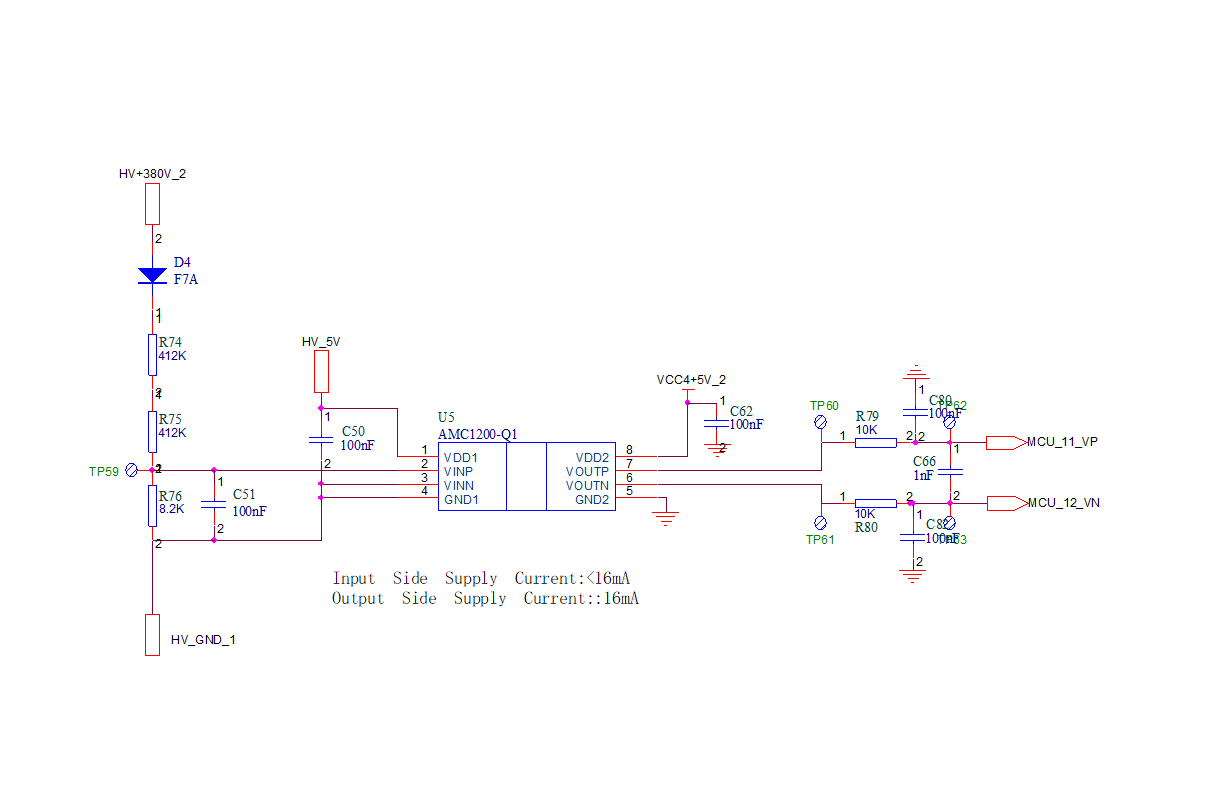
Thanks!
Regards!
Eric
↧
THS4281EVM: This EVM seems to not have schematic attached.
Part Number:THS4281EVM
Unlike other EVM, THS4281 seems to not have schematic attached.
This is too odd that there is no seperate EVM specification document. Instead, only a layout section in the datasheet is provided.
The EVM still lacks schematic and BOM information which usually can be easily found within other device's EVM specification.
By the way, the schematic shown in the first page of THS4281 datasheet looks wrong. The inverting and non-inverting inputs hooking on the sensing resistor's ends should be swapped.
Could you please help clarify these concerns.
Thanks a lot.
↧
THS4271EVM-UG: The user's guide content is inconsistent with what real picture shows
Part Number:THS4271EVM-UG
I was looking into the possibility of taking advantage of the seperate inverting and non-inverting input terminals that THS4271EVM provides. (see the attached picture)

But the user's guide shows that only non-inverting input terminal is exposed.
How to tell which one should be seriously followed?
↧
INA3221: INA3221 Power Valid
Part Number:INA3221
Hi Expert,
The Power-Valid Upper-Limit Register default value is 10.00V and Power-Valid Lower-Limit Register default value is 9.00V during power on reset.
If we change PV limit register value for current design (12V, 3.3V, 1.8V), then this value can be asserted after setting complete until power on/off again.
Am I right?
thanks,
Mark Chen
↧
↧
INA105: Unity-Gain Inverting Amplifier Output Issues
Part Number:INA105
I'm needing some assistance on an application design. I'm trying to invert a 0-10VDC sweep using the INA105 in a Unity Inverting configuration. I'm getting good resrults in Tina-TI and transferred to EasyEDA and got some boards made up. After assembly and powering up with a +-12VDC power supply, i'm getting no reading on my output pin when testing with an input voltage between 0-10VDC. Any help would be appreciated.


↧
LM324-N: Does LM324-N have new version?
↧
PGA113: causing distorted signal on pre-amp circuit output
Part Number:PGA113
Hi all,
I am trying to design a programmable amplifier board. The intent was to be something small with the PGA113 at its heart, being controlled by a PSoC5LP. However, I have noticed that when the gain is set to anything other than unity on the PGA113, there is noticeable distortion on the INPUT signal to the PGA113.
Here is an image of the schematic being used. It is designed with am LM358 preamp with LPF and adding a DC bias at half voltage:

the signal Sig1_Preamp is the signal in question here. I have noticed that when channel 1 on the PGA113 is enabled and the gain is set to 5 or above, what was once a clean signal from the pre-amp circuit becomes noticeably distorted. Those distortions get amplified and are seen on the output of the PGA113. When I disable the channel or switch to the other channel on the PGA113, the signal returns to its normal, clean state. I have more or less followed all of the design recommendations for the PGA113, so I am unsure what exactly could becausing the problem here! It's like the PGA113 is loading the pre-amp circuit despite it having relatively high impedance inputs with very low input bias current!
Any assistance is appreciated.
Some extra info:
Signal input is capacitvely-coupled (ac-coupled) through a 3.3uF cap into the SIG1 input on the schematic. I am using a 100mVpp @ 5kHz sine wave test signal. If I shrink the input to be vanishingly small (so small that it's mostly noise), I can make the lower gain values (2x and 5x) lose the weird noise signal. If it is desired I can provide scope shots with specific input signals.
↧