Quantcast
Channel: Amplifiers forum - Recent Threads
Viewing all 18869 articles
Browse latest View live

Using PSpice model for OPA140 or OPA2140

$
0
0

Hi all,

I am using OPA2140 as my 2nd stage of my transimpendance amplifier (reference: http://e2e.ti.com/support/amplifiers/precision_amplifiers/f/14/t/158884.aspx#584443).  Following the SLOA070 guide, I successfully imported the Spice Model in PSpice and changed it symbol to a triangular shape accordingly.  What I notice when I was changing the symbol is that apart from the familiar OPA2140 sub-circuit, I also see a list of other sub-circuits -- FEMT_0, IDEAL_D_0, IDEAL_D_1, etc.  Surely, because I did not attend to these sub-circuits, a bunch of errors was generated during simulation (as follows):

ERROR(ORPSIM-15108): Subcircuit IDEAL_D_0 used by X_U1.XU12 is undefined
ERROR(ORPSIM-15108): Subcircuit IDEAL_D_0 used by X_U1.XU8 is undefined
ERROR(ORPSIM-15108): Subcircuit FEMT_0 used by X_U1.XIn11 is undefined
ERROR(ORPSIM-15108): Subcircuit RNOISE_FREE_0 used by X_U1.XR109 is undefined
ERROR(ORPSIM-15108): Subcircuit RNOISE_FREE_0 used by X_U1.XR109_2 is undefined
ERROR(ORPSIM-15108): Subcircuit VNSE_0 used by X_U1.XVn11 is undefined
ERROR(ORPSIM-15108): Subcircuit VCVS_LIMIT_0 used by X_U1.XU14 is undefined
ERROR(ORPSIM-15108): Subcircuit IDEAL_D_1 used by X_U1.XU13 is undefined
ERROR(ORPSIM-15108): Subcircuit RNOISE_FREE_0 used by X_U1.XR109_3 is undefined
ERROR(ORPSIM-15108): Subcircuit RNOISE_FREE_1 used by X_U1.XR109_4 is undefined
ERROR(ORPSIM-15108): Subcircuit VARICAP_0 used by X_U1.XU9 is undefined
ERROR(ORPSIM-15108): Subcircuit VC_RES_0 used by X_U1.XU7 is undefined
ERROR(ORPSIM-15108): Subcircuit VCVS_LIMIT_1 used by X_U1.XU5 is undefined
ERROR(ORPSIM-15108): Subcircuit VCVS_LIMIT_2 used by X_U1.XU6 is undefined
ERROR(ORPSIM-15108): Subcircuit VCVS_LIMIT_3 used by X_U1.XU3 is undefined
ERROR(ORPSIM-15108): Subcircuit VCVS_LIMIT_3 used by X_U1.XU1 is undefined
ERROR(ORPSIM-15108): Subcircuit IDEAL_D_1 used by X_U1.XU2 is undefined
ERROR(ORPSIM-15108): Subcircuit VCCS_LIMIT_0 used by X_U1.XU26 is undefined
ERROR(ORPSIM-15108): Subcircuit VCCS_LIMIT_1 used by X_U1.XU4 is undefined
ERROR(ORPSIM-15108): Subcircuit VCVS_LIMIT_4 used by X_U1.XVCVSPSRR is undefined
ERROR(ORPSIM-15108): Subcircuit VCVS_LIMIT_5 used by X_U1.XU22 is undefined
ERROR(ORPSIM-15108): Subcircuit VCVS_LIMIT_5 used by X_U1.XU21 is undefined
ERROR(ORPSIM-15108): Subcircuit VCVS_LIMIT_5 used by X_U1.XU20 is undefined
ERROR(ORPSIM-15108): Subcircuit VCVS_LIMIT_6 used by X_U1.XU19 is undefined
ERROR(ORPSIM-15108): Subcircuit IDEAL_D_0 used by X_U1.XU11 is undefined
ERROR(ORPSIM-15108): Subcircuit IDEAL_D_0 used by X_U1.XU10 is undefined
ERROR(ORPSIM-15108): Subcircuit RNOISE_FREE_1 used by X_U1.XR109_5 is undefined
ERROR(ORPSIM-15108): Subcircuit RNOISE_FREE_0 used by X_U1.XR102 is undefined
ERROR(ORPSIM-15108): Subcircuit RNOISE_FREE_0 used by X_U1.XR101 is undefined
ERROR(ORPSIM-15108): Subcircuit RNOISE_FREE_0 used by X_U1.XR105 is undefined
ERROR(ORPSIM-15108): Subcircuit RNOISE_FREE_2 used by X_U1.XR104 is undefined
ERROR(ORPSIM-15108): Subcircuit RNOISE_FREE_0 used by X_U1.XR103 is undefined

Subsequently, I tried the PSpice model for OPA140, thinking it does not include those extra sub-circuits, but I was wrong.  These sub-circuits seem to be parameters that I can fine tune for my simulation, however, I do not have a proper understanding what each one are.  My search online and in the forum for these parameters came out nothing.  Please let me know if anyone has some insight into this.  Thank you in advance!

- Wayne Chu


Powerline Communications AFE031

$
0
0

Hi,

I want to use an AFE031 for a powerline communication. In my design there is a particularity, the information is going to be mixed with 24Vac instead of 220Vac or 120Vac. My doubt is have I only to change the value of the HV  capacitor or more things to adapt the desing to this AC voltage?

Thanks,

Luis.

Multistage noise voltage calculation

$
0
0

Hi all. I'm calculating the total rms noise of a circuit: what have I to do when I transfer the first stage noise voltage at the output of the second stage? Multiply it for the second stage gain (and sum with the second stage output noise through Pythagorean theorem) ? thanks in advance.

Regards.

Ph electrode and Reference electrode amplifier recommendation

$
0
0

I am using pH[16-705] and reference electrode[16-702] from Microelectrodes.

I need recommendation on instrumental amplifier and voltage buffer amplifier.

Amplifier requirements are:

1) Amplifier application needs to be for Ph measurement

2) Amplifier need to have very very low input bias current, as low as FemtoAmps if possible

3) Amplifier needs to very high input impedance up to 1000 G ohms if possible

3) differential mode configuration for low CMRR

I looked at LMP91200 but it requires a controller to set the gain. I am ok with two different chips and  connect them together as a voltage buffer followed by [differential amplifier with RC filter]. 

Any recommendation would be greatly appreciated.

With the operational amplifier can do two wire, an output also provide 4-20mA, 12-24V, one of the ground

$
0
0

With the operational amplifier can do two wire, an output also provide 4-20mA, 12-24V, one of the ground

XTR111 Basic Connections

$
0
0

Hello Sir,

I am new to designing and have some questions regarding XTR111.

I am currently designing a circuit for highly constant current source for optical purposes using a high precision constant voltage reference as  the voltage source and then XTR111 as the high precision voltage to current converter giving 25mA as the constant current output(Rset= 1k, and voltage reference output as 2.5V).

I wanted to ask you whether how and what connections are to be made at the REGS and REGF pins, and how is the load to be connected.

Thank you in  advance!

Regards,
Pratik Bhamre
Project Asst. Engineer
IIT Bombay

OPA2277 field failures

$
0
0

Looking for input/ideas about OPA2277UA devices failing in the field. Devices have been running for 1-2 years without incident and now we are seeing occasional failures (low percentage). In some devices, both amps have stopped functioning - in others it is just one amp. Ideally we would like to have the failed devices analyzed to try and sort out the root of the problem. We are happy to provide any further information that is helpful.

Thanks,

Mike

How to remove offset from OPA547

$
0
0

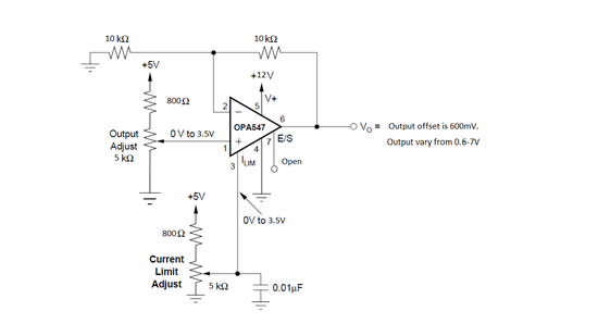
Hello sir,

I want to use the opa547 in my one application & i do not want any offset at output. for testing purpose i have assembled the opa 547 circuit on general purpose board. right now i am providing power supply of +12v w.r.t. gnd & i am getting offset of 600mV. it is clearly written on datasheet of opa547 for VO=0V use -1V on pin number 4. can i use negative voltage reference? Can you please suggest me any -ve voltage reference from positive supply?


AFE032 DAC Digital Filtering configuration

$
0
0

Hi,

The datasheet talks about digital filtering for three bands - CENELEC_A, ARIB and FCC bands.

What configuration needs to be adopted for an application working in all CENELEC bands (A,B,C,D): 35 kHz to 148 kHz with a sampling frequency of 400kHz.

Also, page 31 of the datasheet doesn't mention about which blocks of the DSP path needs to be enabled for a sampling frequency of 400 kSPS.

Please comment on using XCLK frequency of 8MHz. This is the frequency that could be generated by the application processor I use, closely matching the jitter requirements. Does the XCLK need to have exactly 50 percent duty cycle?

What do the default values of the coefficient registers of the Digital filtering blocks signify?

Regards,

Karthikeyan

AFE032 Clock requirements

$
0
0

Hi,


I intend to use the AFE032 in the FCC band with a sampling frequency of 1.2 MHz.

The ARM processor interfaced with the AFE032 runs at 168MHz and can generate signals that are divisions of this.

So, the processor cannot exactly generate 19.2 MHz, which can be divided by 4 for DAC_CLK to be 4.8MHz.

What are my other options here?

Regards,

Karthikeyan

AFE031 SPI Trouble

$
0
0

  I am trying to interface the AFE031 via SPI to control the DAC. The output is changing as I write to SPI but not as I expect. I suspect that the SPI mode is incorrect, is there a way to tell the AFE031 which mode to expect? I have read the data from a logic analyzer and am quite certain that my SPI signal is sending the proper data. Any other info regarding the AFE031 would be very much appreciated as  I find the datasheet and Analog Front End Design Note to be very brief.


 I have attached my code and would appreciate if you could take a look at it. It is very simple

http://pastebin.com/pjkMQaN4

IVC102 with large external capacitors

$
0
0

I'm looking at using an IVC102 amplifier for integrating a current from a PMT. The expected range is within 1 nA - 5 µA and the requested integration times are in the second range. To not saturate the sensor (if I've understood things correctly) I would need to use a large external capacitor to do this (µF). 

Would this be expected to work, considering that my capacitor would be several orders of magnitude larger than the internal ones?

Many thanks and best regards

Mikael

Reliability Forecast for the ISO124 isolator

$
0
0

Hi Everbody,


Currently, we are studying the usage of the isolator ISO124P in our applications. Being in charge of the reliability and safety studies, I would like to know if someone have some reliability models, reliability feedback of this component, ... or something else around this subject to help me to evaluate the reliabilty of thi scomponent in our applications.

In normal cases, I use the IEC62380 standard, but this type of component doesn't exist or is too far from this one.

Thanks by advance.

Best regards,

ACF2101 Problem with low currents

$
0
0

Hi!

I want to use ACF2101 as a photodiode amplifier.

I connect the ACF2101 as in typical connection on Fig 1a in datasheet, photodiode connected only to one channel. I am not using select switch, the supply voltage is +-15 V.

Typical hold pulse duration was about 5 mS, reset 1.5 mS and the reset pulse is shifted by 2.3 mS from the beginning of the hold pulse,  pulse repetition rate 10 Hz, and the integration duration 95 mS.

At low current levels (photodiode was in complete dark, expected dark current about 250 pA) the output of the ACF2101 after starting integration cycle goes up (for about 5 mV in 100 mS), instead of going down to negative voltages, see figures below

Zoomed portion around the end of integration cycle:

Green dashed line is scaled hold signal and red - reset.

When I increase the current the slope of the output signal is decreasing, so at some point it can be flat and when you increase it more it looks something like this:

Zoomed portion around the end of integration cycle:

And the beginning of the integration cycle:

Also here are the timing diagrams of the hold and reset separately:

So my questions are:

1. why does the output voltage goes up at low current levels?

2. why does the voltage drop at the beginning and at the end of integration cycle is so big (around 15 mV)?

and why the drop at the beginning of the integration cycle is positive? (if I understand it correctly it should be negative)

So far I have tested two devices and both channels on those, qualitatively they all behave similar way.

I will be appreciate for any help with this issues,

thank you!

dudas con AFE031

$
0
0

estimated

could help me with the following questions that I have about AFE031.

setting the AFE031 in two-wire mode and connecting directly E_Rx_OUT E_Tx_IN and Tx / Rx USART of MCU. Is it possible to establish an asynchronous serial communication (baud rate 19200)?

the output levels of the PGA of E_Rx_Out can be configured as CMOS outputs?

take as a reference page 33 and 34 of the datasheet

thank you very much for your support!

best regards

Cesar Zicker...


TLV2374 input overvoltage protection

$
0
0

My positive power supply is +5V.  What happens if I apply +9V to the noninverting input through a 127K resistor?  Will the op amp be damaged?  Does the TLV2374 have input ESD protection?  Thanks.

3 way isolation for field interface modules

$
0
0

Hello All,

I intend to design a signal conditioning card for various field signals where I need to give standard 3 way isolation as shown in block dia. :

Input of the card will be 4-20mA signal from various transducers and output should be isolated 0-10V signal.

Here, my main concern is size and cost which I need to restrict to as low as possible.

One possibility can be using small DC-DC converters but it becomes a costly design.

I would appreciate your help if you have worked on something like this and share your ideas with me.

Thanks and Regards

shrikant. 

OPA 547 offset problem

$
0
0

Hi,

I want to use the opa547 in my one application & i do not want any offset at output. for testing purpose i have assembled the opa 547 circuit on general purpose board. right now i am providing power supply of +12v w.r.t. gnd & i am getting offset of 600mV. it is clearly written on datasheet of opa547 for VO=0V use -1V on pin number 4. can i use negative voltage reference? Can you suggest me any -ve voltage reference from positive supply?

PGA 280 wire break and input diconnect detection

$
0
0

Hello ,

We are using the PGA 280 , a few questions  

There are 2 terms mentioned in the  datasheet 

1 >> Wire break detection

2 >>Input disconnection

What is the difference between the two ?

I understand that we need to toggle switches using the registers via SPI to detect these conditions but didnt get much clarity on the sequence of toggling switches (which to close / open and when )reading the data sheet

Could you please explain step by step of doing this

Will be great help .....

Thanks

Abhay

Input current is Very high on LMC660AIM

$
0
0

We have a LMC660AIM that are connected as an ordinary amplifer. Its powered from an 12VDC supply. On the positive input pin we use a 100k serial resistor. The amplifer have a gain of 4 bu feeback resistors from output. On the 100k input resistor we put 2.5V, and have about 10V on the output. Nothing strange about that so far.

The strange thing is that I measure a 20mV drop over the 100k input serial resistor. This means that it will flow about 250nA to the maplifer positive input pin. And this is strange as datasheet say something about a couple of pA.

Why does if flow 250nA into the positive input pin of the LMC660 ??

(we have tried other internal amplifers and samples without any change)

Viewing all 18869 articles
Browse latest View live


<script src="https://jsc.adskeeper.com/r/s/rssing.com.1596347.js" async> </script>