↧
INA128: Offset Voltage

↧
INA128: Power-on Sequence
↧
↧
INA128: Output Voltage for RG Pins

↧
OPA211: PCN#20180221003 Datasheet for OPA211, OPA2211
Part Number:OPA211
Kindly please help to advise below as need to perform qualification urgently.
- When comparing Rev I vs Rev J datasheets, observed that the units for RL, RF, R1, R2 and R3 were changed from Ω to W. Please confirm whether this change is correct or typo error. This change was not stated in TI’s PCN. If this change is correct, please provide the reason for this change.

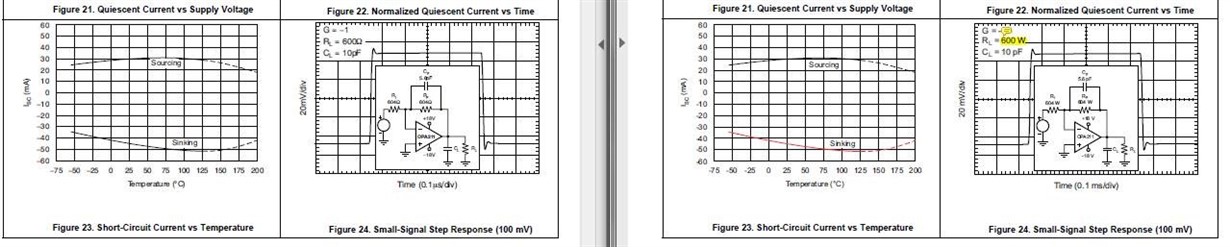

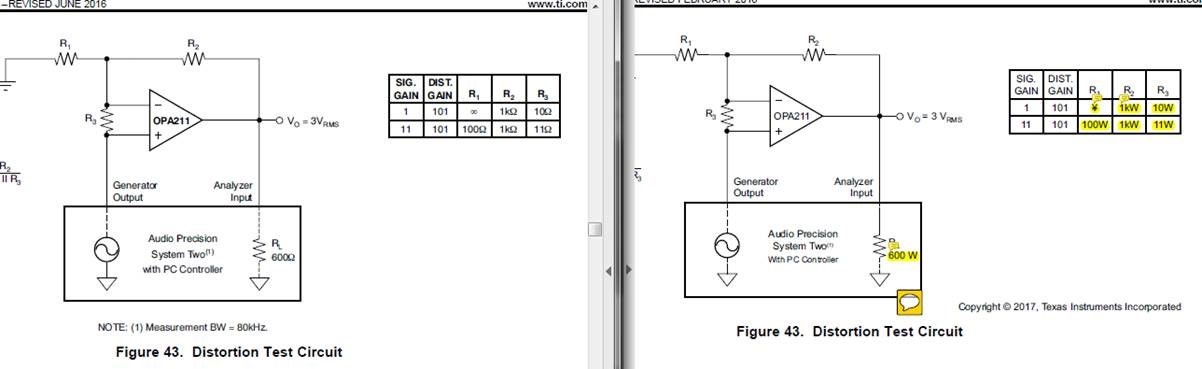
- Observed that the time stated in datasheet has been changed from 0.5µs/div to 0.5ms/div; from 2µs/div to 2ms/div and from 100µs/div to 100ms/div. This change was not stated in TI’s PCN. If this change is correct, please provide the reason for this change. Please advise whether any changes to the components due to this change and what are the risk/impact due to this change.

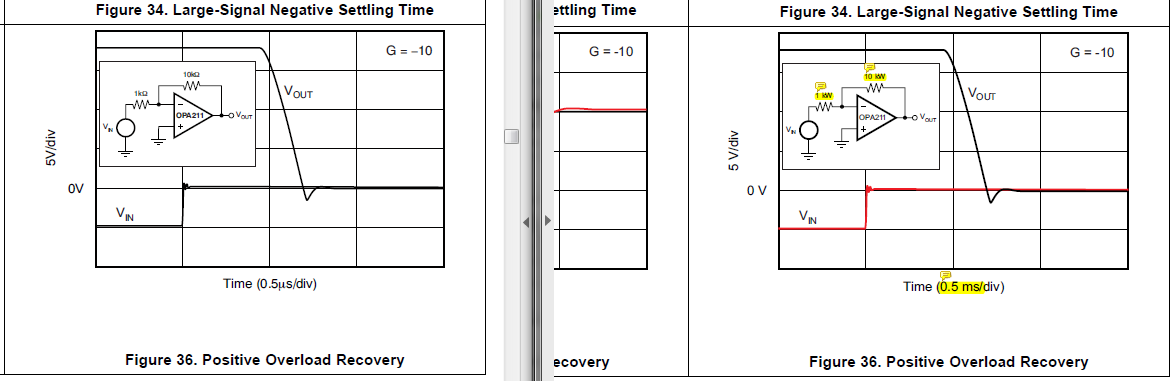

- Observed that below layout has been changed and this is also not stated in TI’s PCN. Please provide the reason for this change. Please advise whether any changes to the components and what are the risk/impact due to this layout change.
![]()

↧
OPA211: OPA211 SPICE model feature at 20MHz
Part Number:OPA211
Hello,
I'm want to use OPA211 to design a low noise amplifier.
However, when I use the SPICE model in the simulator, I see an effect starting from 1MHz (picture is output noise of unity gain buffer for reference).
When I looked into the SPICE model, it states"INPUT VOLTAGE NOISE WITH 1/F AND FEATURE AT 20 MEGAHERTZ" .
What is this feature? I don't see anything in the datasheet of the opamp about this effect?
Thanks,
Sven
↧
↧
PRECISION SIGNAL AMPLIFY AND REMOVE DC OFFSET
Hi.
I want digitize a weak signal .
that signal come out a inductive sensor.signal have dc offset equal battery voltage.
insert a picture from out put of sensor.

in past Zak Kaye recommended a circuit.but i do't understand what circuit is best and why??
↧
OPA827: The output voltage question for OPA827
Part Number:OPA827
Hi team,
I have a question for 5.1. TI Precision Labs - Op Amps: Bandwidth 1. In this video, the input signal frequency is 200kHZ, the closed gain
is set to 100V/V. The GBW for OPA827 is 22MHZ. So, 200kHZ*100V/V=20MHZ<22MHZ, So, the 200KHZ input signal can be
normally amplified 100 times. That is when the input signal is 200KHZ, the closed gain should be 100V/V, correct?
But in TINA circuit, it shows the closed is 37.75dB when the input signal is 200KHZ. Would you explain this?

↧
INA148: to set the tolerance for offset and Gain on pspice model
↧
OPA4196: TSSOP Package?


↧
↧
CCS/OPA4140: OPA4140 overcurrent
Part Number:OPA4140
Tool/software: Code Composer Studio
Dear TI officer and members,
Currently, I am using the CC2541 to collect an analog signal.
The amplifier of OPA4140 was adapted as shown in the listed figure.
Here is the problem that the OPA4140 is every hot (close to 80 C in the ambient environment of 25 C) due to the large input current of 120 mA, which is overcurrent.
This is impossible under the normal condition. I can not find the reason. Please help me.
The positive and negative voltages are provided by TPS65133 dual-output supply.

Best regards,
Derrick
↧
LMP7721MAEVALMF_NOPB: LMP7721MAEVAL
Part Number: LMP7721MAEVALMF_NOPB
I want to know if it's available the LMP7721 Evaluation Board but just the PCB without components.
↧
LMC6082: LMC6082IMX/NOPB
Part Number:LMC6082
HI Team,
By Mistake I inserted the OP-AMP IC component in the socket in the reverse direction, and after testing it on the fixture circuit (voltage follower input Vref=2.5V), I measured the same 2.5V on OP-AMP1 and 1.71V on OP-AMP2. which means one side of OP-AMP got failure, is that because of reverse direction insertion?
Based on the pin out of the device I would expect if the device was placed in the reverse direction would expect both devices in the package to Fail?
Please clarify the query...
your immediate response would be highly appreciated.
Thanks.
Prakash H
↧
OPA333: Auto-zeroing function and auto calibration function
Part Number:OPA333
Hi all
Would you mind if we ask OPA333?
<Question1>
What is the difference auto-zeroing function(OPA335) and auto calibration function(OPA333)?
Is that the same?
<Question2>
In relation to <Question1>, in case of auto-zeroing = auto calibration, on the following document, about the figure Auto zero(OPA335), there are some SWs.
http://www.tij.co.jp/jp/lit/an/jaja017/jaja017.pdf
On OPA335's datasheet, there is the description "This amplifier is zero-corrected every 100µs using a proprietary technique."
So, it occurs switching operation every 100us, right?
<Question3>
If you have the detail content of auto-zeroing function(and auto calibration function), could you give us it?
<Question4>
Does Auto-zeroing function(or auto calibration function) have any temperature effect?
The customer will use the device with following temparature condtion.
Temparature range : -30C~60C
So, if you have some temperature characteristics for this function, could you give us it?
<Question5>
The customer are looking for zero drift amp without auto-zeroing function or auto calibration function.
If you have know these devices, could you let us know?
(We assume that it doesn't exist.)
Kind regards,
Hirotaka Matsumoto
↧
↧
XTR115: XTR115
Part Number:XTR115
Hi,
I am using XTR115 for conversion of PWM to 4-20mA.In which I will give 0 to 2.2 V at input resistance of XTR115 , using Input resistance and resistance between Vref and Iin pin I will control 40-200uA current at input side.I get correct result when I connect load resistance 100E or less than 100E but not get correct result when load resistance geter than 100E. So kindly guide me how to choose load resistance and what is minimum and miximum load resistance I can connect at output side.
↧
TINA/Spice/LMP7721: LMP7721 input capacitor
Part Number:LMP7721
Tool/software:TINA-TI or Spice Models
Dir Sir/Miss.
From LMP7721 specification, it tells me that the typical input capacitance of the LMP7721 is about 11pF, and I have download the spice model and run some simulation, I'm not sure whether the model has build this input capacitor in? and the capacitors are connecting between the inputs and the V- pin right?
Thanks
Jack
↧
TINA/Spice/TLE2027AM: Query about spice model listing given in datasheet
Part Number:TLE2027AM
Tool/software:TINA-TI or Spice Models
Hello,
I am using a TLE2027 op-amp in several places in one of our products. I would like to use a spice simulation of one or more of these circuits. The datasheet "SLOS192C− FEBRUARY 1997 − REVISED APRIL 2010" , page 33, contains a listing of a spice model which I copied from the datasheet into my spice circuit. I have also included it below. Unfortunately the TLE2027 model does not run because it is not complete. There are instances of a diode called 'dz' but there is no definition of what dz is. By contrast, there are also diodes called 'dx' and there is a line towards the end of the sub-circuit that defines what dx is.
If I edit the model to change all the instances of dz to dx, I can make the model run, but it doesn't match what was written in the datasheet! Is this hacked model trustworthy?
Is a more recent spice model of the TLE2027 available?
I tried looking at TINA for a spice model but when I opened up the TLE2027 component there I found a sub-circuit (.SUBCKT) for a TLC27L2. That doesn't look right. The TLE2027 has bipolar inputs and the TLC27L2 is CMOS?
Editted to add
Forgot the spice model:
.subckt TLE2027 1 2 3 4 5
*
c1 11 12 4.003E-12
c2 6 7 20.00E-12
dc 5 53 dz
de 54 5 dz
dlp 90 91 dz
dln 92 90 dx
dp 4 3 dz
egnd 99 0 poly(2) (3,0) (4,0) 0 5 .5
fb 7 99 poly(5) vb vc ve vlp vln 0 954.8E6 -1E9 1E9 1E9 -1E9
ga 6 0 11 12 2.062E-3
gcm 0 6 10 99 531.3E-12
iee 10 4 dc 56.01E-6
hlim 90 0 vlim 1K
q1 11 2 13 qx
q2 12 1 14 qx
r2 6 9 100.0E3
rc1 3 11 530.5
rc2 3 12 530.5
re1 13 10 -393.2
re2 14 10 -393.2
ree 10 99 3.571E6
ro1 8 5 25
ro2 7 99 25
rp 3 4 8.013E3
vb 9 0 dc 0
vc 3 53 dc 2.400
ve 54 4 dc 2.100
vlim 7 8 dc 0
vlp 91 0 dc 40
vln 0 92 dc 40
.modeldx D(Is=800.0E-18)
.modelqx NPN(Is=800.0E-18 Bf=7.000E3)
.ends
↧
TINA/Spice/OPA1611: TINA-TI transient simulation fails after reaching 90%
Part Number:OPA1611
Tool/software:TINA-TI or Spice Models
I am simulating a differential amplifier that uses composite amplifier techniques using an OPA1611 and THS4031, and I am looking at the step response stimulating using a 50Hz square wave and simulating from 9.999 ms to 10.001 ms to look at time domain response.
The model has been simulating just fine, but I tweaked some values, and now the simulation will not complete. It hangs at the 90% level. The preview button does not display any useful information, inly displaying a since vertical line from -730u to 590u at 9.01 ms (which should not be part of the simulation).
How do I trouble shoot these types of issues in TINA-TI?
↧
↧
LMC6484: LMC6484 Spice Model
↧
TINA/Spice/OPA454: OPA454 PSPICE model does not simulate flag output correctly?
Part Number:OPA454
Tool/software:TINA-TI or Spice Models
The flag behavior in the PSPICE model dated 2011 asserts the flag output high when a fault occurs.
A more recent data sheet (2016) describes the flag as follows:
The Status Flag is an open-drain active-low output referenced to E/D Com. This
pin goes active for either an over current or over temperature condition.
The model looks like it behaves as an active high output. Which seems to be in agreement with the 2008 data sheet (fig 43-50, 68).
The 2016 data sheet also seems to be wrong everywhere except the pin functions table on page 3.
It seems the data sheets are wrong and the PSPICE model is wrong if the 2016 pins function table is to be believed.
If this is the case then can enable be connected to flag for some more protection, as is the case with the nearly identical LTC6090?
Or would the current limiting function just create conditions for enable oscillation?
Also, is there an update for this model?
Thanks.
↧
OPA4140: The output voltgae problem for OPA4140
Part Number:OPA4140
Hi team,
The customer uses OPA4140 to design an instrumentation Amplify circuit and a voltage follower circuit.
Please check his TINA circuit in the attach.
1. In his actual circuit, if the customer remove the high-pass filter circuit (that is C12,C13 and R32 ),
the figure 1 is VF1 waveform. the figure 2 is VF3 waveform. From the VF3 waveform, there is some glitch waveform.

Figure 1 VF1

Figure 2 VF3
2. If the customer adds the high-pass filter circuit, the figure 3 is VF1 waveform. the figure 4 is VF3 waveform.
Compare to figure 3 and figure 4, the customer found the VF3 waveform moves down than VF1 waveform.

Figure 3 VF1

3. If the customer change R32 to 3K. Figure 5 is VF3 waveform. The amplitude of VF3 moving down is reduced.

Figure 5 VF3
4. If the customer keep R32 be 32k and remove C12 and C13, the VF3 waveform will not move down and
keep the same with VF1.
5. If the customer adds the amplitude of VF1, VF3 waveform will be moved down.
6. If the customer uses OP27 as the voltage follower circuit, VF3 will waveform will not move down.
Would you explain why VF3 waveform can be move down?
(Please visit the site to view this file)
↧