↧
INA321: -
↧
INA321: Shutdown Pin and reference pin
Part Number:INA321
Hey,
I would like to what connections should be made for shutdown and reference pin
↧
↧
XTR111-2EVM: Cannot obtain current
Part Number:XTR111-2EVM
I have just bought a XTR111 EVM board. However, I have encountered several problems with the board.
I have followed the procedures for the basic EVM configuration. But, I still cannot obtained a current output of 4 to 20 mA with the voltage input of 0 to 5 V.
The supplied voltage is +24V as per mentioned in the user guide. I
↧
OPA1632: Stabilization Resistor
Part Number:OPA1632
Hi,
Could you please give me your advice regarding the following stabilization regsistors of R21 and R22 ?
Q1. Optimum value of stabilization resistance
It seems that the resistors(40.2Ω) of R21 and R22 are added to stabilize the feedback loop.
So, could you please tell me how to optimize the value for them ?
Q2. Optimum value of isolation resistance
The resistors of R21 and R22 become the isolator if swapping R21 and R22 with R7 and R8 as below.
I also consider the feedback loop is stable.
So, is OPA1632 able to be applied how to use mentioned above ?

Best regards,
Kato
↧
OPA1642: Low-Noise OPA1642 Pre-amp
Part Number:OPA1642
Hi,
I'm working on a product that requires signal conditioning of an audio signal from a wide variety of sources to under 3 V peak (for the input of an ADC). Technically the full-scale input should be about 1.15 V peak but in order to avoid damaging the ADC it must be kept under 3 V peak. Noise should be kept to the minimum possible.
To accomplish this, I designed this schematic using the OPA1642 audio op amps. The input stage is set up as a unity buffer with a bootstrap for high input resistance. The second stage is set up to provide gain anywhere from 1/10*Vin to 333*Vin. Finally the output is clamped to about +/- 2.5 V to protect the ADC.
The idea is that the user will be able to adjust the gain to maximize the ADC's resolution.
I'm looking for general feedback on the design of the circuit as I've never attempted something like this. It seems to work well in simulations. One problem I've noticed is that the second stage contributes a lot to the noise output in simulations when the pot (R6) is turned up (output~250 nV/root-Hz). Oddly enough, R4 is shown to contribute the most to the noise output in the simulation, where I would have expected R6 to be the noisiest at high values. I'm not sure how to get the range of gain I need with less noise though.
Any help, pointers, criticisms are much appreciated!

↧
↧
AMC1100: AMC1100 with 4-ch ADC
↧
INA166: High-gain single-power-supply preamp for MEMS microphones
Part Number:INA166
Hello,
This is my first post to the E2E forum.
I'm looking for a way to high-gain amplify the audio signal from a MEMS microphone. I'm presently using SPW2430 MEMS mic on this breakout board for testing, but wish to eventually switch to an AKU350 for its better performance. I have identified TI's INA166 as potentially suitable My microphones have a Vout (an AC signal) and a GND. My question are:
1) The example amplifier circuit in the INA166's datasheet indicates Vin- and Vin+ connected to pins 4 and 5 of the INA166. Does this mean the Vout of my MEMS mic should be connected to the Vin+, and the GND of the Mic Vin-?
2) I would like my preamplifier to run on a single battery; the MEMS mic requires 1.8V, so a single cell 3.7V LiPo battery would be ideal. The example amplifier circuit for the INA166 indicates V+ and V- supplies connected to pins 11 and 6 of the IC. Would you recommend a step-up from my 3.7V supply to something like 12V (possibly using something like TI's TPS61041DBVRG4), and implement a single-supply design (with a virtual ground at the 1/2-way point of GND and my 12V VCC, as described here)?
Thank you!
Ali
↧
OPA2134: Setting the gain of a preamplifier for MEMS microphone
Part Number:OPA2134
Hello,
I'm using TI's OPA2134 and TL072 OpAmps to amplify the audio signal from a MEMS microphone. Schematic and board designs are here. I am looking for very high gain; R2 is a 100K pot; I expect R2/R1 to be the gain for the 1st channel of this preamp. JP1 and JP2 are this MEMS microphone breakout board, and IC3 is a 5V regulator for powering the MEMS microhpone breakout board. The battery is a 12V A27.
My questions are:
1) I find the circuit doesn't work unless the R2 pot is turned to its highest setting, no matter what the value of this pot is. I've tried a 10K, 20K and 100K pot; all appear to produce the same gain, and only work at their highest setting. How do I get better/variable gain out of this design?
2) Are there better (higher gain, lower noise, lower power consuption) ICs for this task?
3) How can I reduce the power consumption of this board to allow for longer battery life?
Thank you,
Ali
↧
Low Cost OPAxxxx Solution for Audio Line Driver
Hi,
Could you please give us your advice since we would like to replace DRV632 with the low cost audio opamp(OPAxxxx series) ?
We are consider to apply OPAxxxx to the multi-feedback(MFB) with differential input which the pwm modulator outputs are input.
The requirements are shown as below.
<Requirements>
- VCC : 3.0 ~ 3.6V
- diferential input signal : pwm modulator pulse
- load impedance : 5kΩ ~ 10kΩ
- without mute pin
- without shutdown pin
- unity gain stable
- low cost
- filter topology : 2nd-order active low pass filter(multi-feedback)
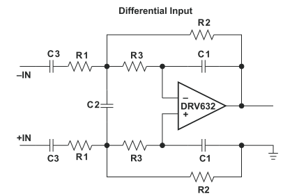
Best regards,
Kato
↧
↧
TLC2254: Dispersion of the equivalent input noise voltage
Part Number:TLC2254
Hi,
The large noise is happened on my customer's circuit.
Could you tell me the dispersion of the equivalent input noise voltage@10Hz/1kHz or 1σ and 3σ of this item?
Best Regards,
Kuramochi
↧
LOG104: Data sheet "Fig8 Precision Current Inverter/Current Source" offset error
Part Number:LOG104
Hi,
I would like to ask you a question about LOG104 application circuit, datasheet Page7 Fig8.
The circuit is designed with OPA2335.
My customer has been evaluating this circuit and get "16uA" output even though input current is "0A". (photodiode is off)
I suppose the output 16uA seems to be made from offset Bias current of OPA2335. Is my idea correct?
If yes, could you adivce me how to adjust it?
Or is this circuit designed output current range specification "from 10nA to 1mA"?
Thank you for you support.
Best Regards,
↧
OPA211: OPA211 Output Current
Part Number:OPA211
Hi All,
I am using an OPA211 for a robotics application in a non-inverting VCCS configuration and had some questions about the output current characteristics. The load is primarily inductive and resistive and also highly nonlinear. The load impedance is low enough 3.5V headroom is maintained on the positive side and 2.5V on the negative side. COMP is some frequency compensation for stability and transient response.

The datasheet indicates typical values @25C for short circuit sinking and sourcing currents (-45mA and +30mA) as well as a graph (figure 23) of how both of these values vary with temperature. Since my application will have symmetrical maximum current, I am concerned only with the lower of the two limits (in this case sourcing).

It also provides a figure relating the maximum output current to the available voltage headroom shown below:

Over let's say 0-150C temperature range the two graphs seem to suggest different sourcing capabilities:
Figure 23 would suggest ~26.5mA based on the performance right at 150C
Figure 37 would suggest ~32mA based on the 3.5V headroom I maintain, also at 150C
My first question is: what is the reason for this apparent disagreement between the two ratings? Is there a difference in input overdrive in the test conditions that I am missing?
----------------------------------------------------------------------------------------------------------------------
My second question is essentially, _roughly_ how much could I expect [whichever of the above 2 potential current ratings I should abide by] to vary from chip to chip? Since minimum and maximum values are not specified in the datasheet I was going to assume that it may vary extremely. I am not looking for any guarantees and no one's safety is riding on this circuit, just inconvenience for me. I am simply looking for a reasonable rule of thumb or ballpark guess from the actual makers of the device to help determine a sensible amount of margin to give myself in this design.
Help is much appreciated, thank you.
↧
PGA112: PGA112: Will the PGA112 or other PGA be suitable for driving a low bandwidth signal into the THS4551 into a 24-bit Sigma Delta ADC?
Part Number:PGA112
I have been evaluating the ADS127l01 (24-bit delta sigma adc) for the purpose of digitizing frequencies in the ~10-250 Hz bandwidth from a geophone
The eval board for the ADS127l01 drives the ADC with theTHS4551 differential amplifier. I am aiming for a dynamic range of 120 dB, 20 ENOB. (understandably idealistic goal)
This adc is being tested for portable, low power instrumentation and the wide band filter option is particularly useful. The cost per unit for the ADS1282 (seismic conditioning ADC with PGA, sinc filter, wideband filter etc.) is is too high for the volumes I need, Nevertheless, it is a phenomenal ADC+PGA for my application.
My price point requires an external PGA or at the very least a high quality fixed gain Operational Amplifier (I have been looking at the OPA330)
I have a few questions regarding this application:
1. Is the PGA112 a good choice to go directly into the THS4551 to drive the ADS127L01? If not, would more aggressive active filtering with the THS4551 cause a significant improvement?
2. Is there a PGA the fine T.I. engineers would recommend for my application?
3. One solution that comes to mind is the INA333 with a digitally controlled variable resistor, would this provide resolution and quality for driving the THS4551?
4. The OPA330 geophone preamplifier looks promising for a fixed gain amplification. Am I correct in this assumption? I would power the OPA330 with a single supply and apply 20x gain. DC shift between the rails and drive the THS4551. Would this solution be conducive to success?
Thank you,
Sorry for so many question.
↧
↧
OPA334: testingform
Part Number:OPA334
This is only a test of the form
↧
Compiler/OPA104: testing...
↧
Linux/OPA333: TEST production
↧
LMP91000: LMP91000
Part Number:LMP91000
I am using the LMP91000EVM connected to a Raspberry Pi microcontroller, to read H2S gas concentration. This is for a senior design project at LeTourneau University.
I have successfully set the I2C registers to configure the board, and I have read the SPI output from the board successfully to the Pi. At the bottom of this email is what I am reading as the output from the board.
I am unsure how to interpret this data, as it seems to typically be interpreted by the LMP9xxxx Sensor AFE Development Sofware/Hardware Platform on a laptop. However, since I am using the Pi to read the data directly, I am curious how to interpret the data. Is the output a hexadecimal code, representing concentration? If not, what processing is done to the SPI output of the LMP91000EVM to calculate concentration?
Thank you, and I look forward to hearing from you soon.
Example output:
[2, '\x00 ']
[2, '\x00;']
[2, '\x002']
[2, '\x00:']
[2, '\x00I']
[2, '\x00N']
[2, '\x00K']
[2, '\x00G']
[2, '\x00G']
[2, '\x00J']
[2, '\x00K']
[2, '\x00J']
[2, '\x00G']
[2, '\x00I']
[2, '\x00J']
[2, '\x00I']
↧
↧
LMC662: LMC662 600ohm drive
↧
INA321: Range of Negative Power Supply
↧
AFE031: HOW MANY NODES AND CABLE LENGTH
↧